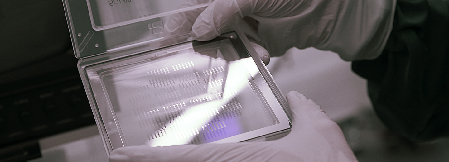
Structure formation
Micro- and nanofabrication for structuring a wide range of materials down to 5 nm on substrate size up to 4'' in size
Keywords and applications
Keywords
Nano and micro fabrication, electron beam lithography, focused ion beam lithography, photolithography, imprint lithography, dry etching, wet etching, thin-film deposition, spin coating, epitaxy
Applications
Nanotechnology, nanoelectronics, life science, nanophotonics, microfluidics, energy storage, optical devices, MEMS
Profile
We offer a micro- and nanofabrication platform to structure a wide range of materials down to 5 nm on substrate size up to 4’’ in size. In addition, provide a selection of state-of-the-art process equipment for lithography, etching, thin-film deposition and epitaxy. Finally, we have expertise and research focus in solar cells, sensors, microfluidics, nanomarkers and plasmonics, among others.
Services
Nano and micro fabrication from macro to nanoscale.
Available techniques
- Electron Beam Lithography (EBL)
- Focus Ion Beam Lithography (3 ion beams)
- UV photolithography
- Physical Vapor Deposition (PVD)
- Silicon Dry Etching (ICP-RIE)
- Molecular Beam Epitaxy
Labs & Equipment
Cleanroom
- Scanning Electron Microscope Hitachi S-4800, Raith EBL extension
- Orion NanoFAB, Helium Ion Microscope, He+, Ne+, Ga+ focused ion beams
- Mask Aligner, Karl Suss MJB4
- PVD system Cryofox Explorer 600
- Spin coater RRT Lanz EBS 11
- Adhesion promoter Yield YES LP III
- Dry Etching (ICP-RIE) Alcatel AMS110 SE
- Wet Etching
- Plasma Asher LFE 120 Barrel Plasma System
Contact
Jacek Fiutowski
Associate professor, PhD
SDU NanoSYD
Mads Clausen Institute
T +45 6550 1678
fiutowski@mci.sdu.dk